Stories about laser weapons usually begin with a large beam director and high power. Yet the light can start in a semiconductor chip no bigger than a grain of rice. That chip is a laser diode (LD), the part that pumps fiber lasers and solid-state lasers.
What does the inside of such a small chip look like? This article takes the chip apart into layers and faces. It walks through the active layer where light is born, the waveguide that holds that light, and the facets that serve as mirrors. Then it follows why the beam spreads differently in two directions and where chips tend to fail.
A laser tinier than a grain of rice
In the autumn of 1962, research sites in the United States each showed a working semiconductor laser for the first time, independently of one another. They were two General Electric sites, IBM's Watson Research Center and MIT Lincoln Laboratory. The IEEE milestone describes a device no bigger than a grain of rice that runs on direct current. Today it shows up everywhere, from precision measurement to data storage and communications.
Numbers make the size clearer. In a single-emitter chip, which has only one spot that gives off light, the optical resonator that feeds light back is usually less than 1 mm in any direction. That figure comes from a guideline that the U.S. space agency, NASA, wrote for testing laser diodes for space use.
The basic action is the same as in any diode. When forward current flows through the junction where p-type and n-type semiconductor meet, charge carriers that enter the junction region can recombine and give off light. With strong enough current, a population inversion forms and stimulated emission takes place. That process is covered in "Pump diodes: the part that turns electricity into light".
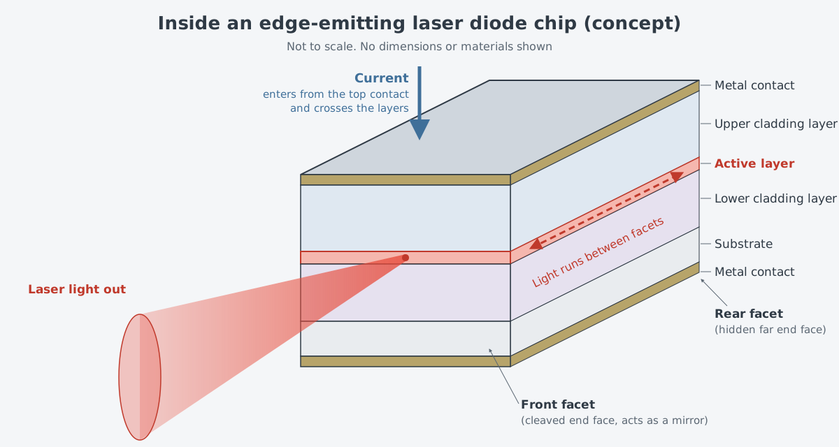
This article looks at where on the chip that action happens. Current enters through metal contacts on the top and bottom and crosses the layers. Light runs at right angles to it, along a thin layer, back and forth from one end of the chip to the other.
The active layer: a thin sheet where light is born
The part of the chip where light is actually made is called the active layer, or active region. It is very thin. A NASA guideline on high-power laser diode arrays says the active region, where heat is generated, is only about 1 µm wide. Light and heat come from the same place, a point that matters again later.
The material sets the color of the light. Making mobile electrons and holes in a semiconductor takes a certain amount of energy, and that amount is the bandgap. A semiconductor gain medium can be designed through its bandgap, which allows a flexible choice of the emitted wavelength.
A textbook on ultrafast lasers lists which semiconductor compounds cover which wavelength ranges. AlGaAs covers 800–870 nm, InGaAs 870 to about 1150 nm, InGaAsP the 1.5 µm range and GaInAsSb 2–3 µm. Adding phosphorus to the GaAs family of materials opens the bandgap into the visible, which makes red diode lasers possible.
Turning bulk semiconductor into a very thin layer changes the number of dimensions in which charge is confined. If bulk material is three-dimensional, a quantum well, a thin layer that traps charge, is two-dimensional.
As semiconductor lasers grew into commercial products, many research groups worked on the quantum well laser. InGaAs layers grown on a GaAs base raise the gain of the quantum well and move the bandgap into the 1 µm region. This material system has served diode lasers for many years.
How thin is thin? In devices built with the same semiconductor layer technology, such as saturable absorber mirrors (SESAMs), a quantum well is typically around 10 nm thick. The value differs from chip to chip, but it gives a sense of a world built from layers measured in nanometers.
The double heterostructure: trapping charge and light together
The first semiconductor lasers of 1962 were p-n homojunction lasers. The Nobel Prize in Physics 2000 background notes that their efficiency was not very high and that they needed a fairly large current to turn on. As a result, running continuously at room temperature was hard.
The answer was to stack different materials. A semiconductor made of several thin layers with different bandgaps is called a heterostructure. The layers range from a few atomic layers to micrometers thick, and gallium arsenide (GaAs) with aluminum gallium arsenide (AlGaAs) is a typical pair. The layers are picked so their crystal structures match, which lets charge move almost freely across the boundaries.
A double heterostructure places a thin layer with a smaller bandgap between two layers with larger bandgaps. This does two things at once.
- Charge gathers. Electrons and holes in the inverted state collect in the middle layer with the smaller bandgap, and hardly any recombination happens outside it.
- Light gathers. The middle layer with the smaller bandgap also has a higher refractive index. So it acts as an optical waveguide that holds the light, and the light lost in the outer layers becomes negligible.
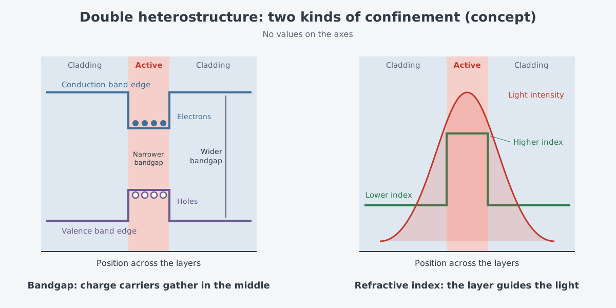
One way to picture it is rainwater collecting at the bottom of a valley, with charge collecting in the middle layer. In reality, weight has nothing to do with it; the different bandgaps of the layers are what hold the charge. On the light side, the idea matches an optical fiber, whose higher-index core keeps light inside. The fiber side of the story is in "How a fiber guides light: core and cladding".
With charge and light in the same layer, the threshold current needed to switch the laser on dropped sharply, and the laser could run continuously without extra cooling. The principle was proposed independently in 1963 by Zhores I. Alferov of the Ioffe Institute in the Soviet Union and by Herbert Kroemer, then at Varian in the United States. Room-temperature continuous operation was reported in 1970, by an Ioffe Institute team in May and a Bell Labs team in June.
Semiconductor lasers that could stay on at room temperature became the basis that made fiber-optic communication practical. One half of the Nobel Prize in Physics 2000 went to these two scientists "for developing semiconductor heterostructures used in high-speed- and opto-electronics."
Facets: cleaved crystal faces become mirrors
A laser needs a resonator. Many lasers build one from two mirrors. A laser diode does not need separate mirrors.
The refractive index of a semiconductor is very different from that of air. Because of this, the face of a semiconductor crystal can reflect enough light to act as its own resonator. The NASA guideline describes this resonator as formed by the cleaved end facets of a piece of semiconductor. These end faces, made by splitting the crystal, are called facets.
Each chip has two facets. Light grows as it travels along the active layer between the rear facet and the front facet, and part of it passes through a facet and leaves the chip.
Cleaving the crystal also played a large role in production. A cleaving technique from IBM's semiconductor laser team greatly simplified the process of making laser diodes in large numbers.
Light from the edge, light from the surface
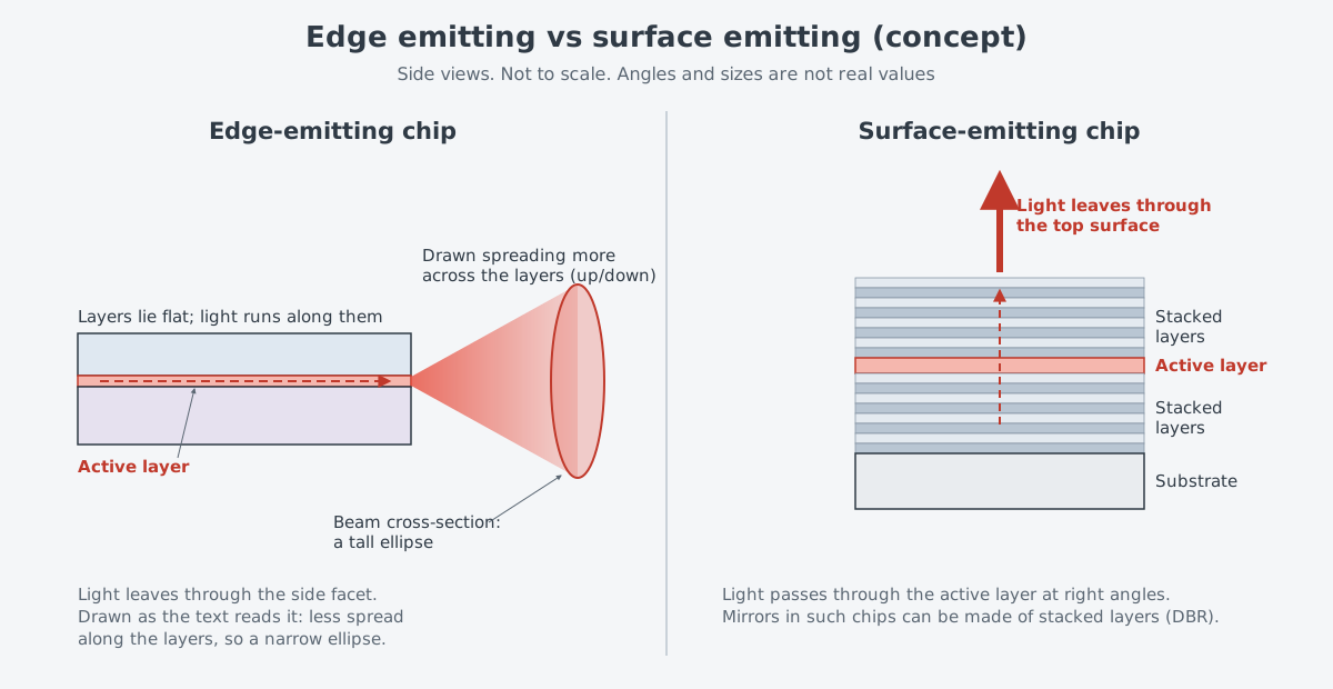
The chip described so far gives off light from the edge of its side face. It is called an edge-emitting laser. Light travels a long way along the thin active layer and then leaves through a facet.
Other chips give off light from their top surface. A vertical-cavity surface-emitting laser (VCSEL) sends its light out through the surface that lies at right angles to the active layer, not through the edge of the layer. Such chips need the thickness of many layers controlled at the level of atomic layers. In vertical-emitting semiconductor lasers such as the optically pumped surface-emitting laser (VECSEL), the beam travels perpendicular to the quantum well gain layers.
Surface-emitting chips build their mirrors from layers, too. Take a VECSEL. Its distributed Bragg reflector (DBR), made of alternating AlAs and GaAs layers, has a high refractive index contrast, so a few layer pairs already give high reflectivity. A VCSEL that works as a chip alone, without an external mirror, is normally pumped electrically.
Both kinds have been made in large numbers for a long time. The Nobel Prize in Physics 2000 background said that edge-emitting lasers and VCSELs were being made at a rate of hundreds of millions a year. CD player lasers led in number of units, and communication lasers led in value.
Why the beam spreads into an ellipse
Test values for high-power diode arrays in the NASA guideline show that the light spreads differently depending on direction. The guideline measures the beam divergence of the whole array's beam in two directions. The typical value is about 10° parallel to the long direction of the bars and about 40° perpendicular to it.
The bars lie in the plane of the layers, so the direction perpendicular to the bars is the direction across the layers. The active layer that gives off the light is very thin in that direction, which helps explain the difference. A beam that starts narrow spreads quickly. "Why a beam spreads: divergence, focus and aperture" explains this relation through the Rayleigh length.
When the spreading angle differs between two directions, the cross-section of the beam stretches one way. Unlike a flashlight that makes a round spot on a wall, the light pattern a short distance from the chip becomes a flattened ellipse. The long side of the ellipse lies in the direction across the layers.
Where chips fail: facets and heat
The NASA guideline names catastrophic optical damage (COD) of the semiconductor facet as the most obvious failure in high-power laser diodes. It adds, however, that COD is not the primary cause of failure.
COD starts at the facet. When laser light is absorbed at the facet and heats it, a thermal runaway follows, and that causes COD. Temperatures can rise by several hundred degrees, melting the facet and stopping the laser.
Facets are not the only weak spot. Bond wires, the fine wires connected to the contacts, can fail, solder can creep or come loose, and the laser bar material can have defects. There is also gradual aging, in which the light output slowly drops and more and more current is needed to keep the same output.
Heat runs through all of this. The active layer where light is made is also the place where heat is made.
Some arrays run in quasi-continuous-wave (QCW) mode, where the current is pulsed on and off. For these, the NASA guideline says excessive heating and thermal cycling of the active regions play a key role in limiting reliability and lifetime. This is especially true for long pulses. So thermal management around the chip deserves attention along with the chip's structure.
These chips are also used in defense. Laser diodes in the 0.8–1.06 µm range are used to pump erbium-doped fiber amplifiers, double-clad fiber lasers and solid-state lasers. Those lasers go into telecom, aerospace, military and medical equipment. How defense laser companies describe their pump diodes is covered in the pump diode article.
What to read next
- "Diode Bars and Stacks: Grouping Chips for More Power": how the chips in this article are lined up in rows and stacked.
- "Pump diodes: the part that turns electricity into light": how light from these chips becomes the pump light for fiber and solid-state lasers.
- "Why a beam spreads: divergence, focus and aperture": why a beam that starts narrow spreads quickly.